The emitter properties play an important role on the c-Si solar cells performance. The high doping concentration at the surface and a deep emitter is potentially beneficial due to the lower contact resistance. However, the increased recombination and degraded quantum efficiency for the high doping concentration are undesirable. While the decreased doping concentration at the surface and a shallow emitter would result in the deteriorate Fill Factors. A selective emitter (SE) technique is developed in the standard screen-printed crystalline Si solar cell. Such a cell features a spatially inhomogeneous emitter, where a high doping level is applied under the front side metallization, resulting in the lower contact resistance and the higher fill factors (FF), while the lower doping level between the contact fingers is adopted, resulting in the less Auger recombination and the better surface passivation. Therefore, a better blue response with higher Jsc and higher Voc values will be addressed. However, most of the proposed processes exhibit several additional steps to pattern the selective emitter, which is detrimental to cost. Moreover, the screen printed Ag gridlines should locate above the selective emitters, which poses strict alignment requirements.
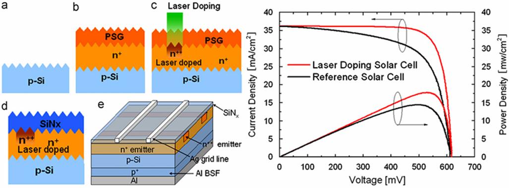
Nowadays, Prof. WAN Qing’s group from the Ningbo Institute of Materials Technology and Engineering (NIMTE), Chinese Academy of Sciences (CAS) has made a progress on the selective emitter processing. They have successfully developed a novel front metal contact patterning scheme for crystalline silicon (c-Si) solar cells. The innovative laser patterning process features only a single additional step compared to conventional silicon solar cell work flow. Subsequently to the furnace diffusion, the selective highly doped phosphorus emitter was formed by using the laser doping process with the phosphosilicate glass (PSG) layer as the precursor layer by using the laser with 532 nm wavelength, which produced selective emitters. The front and back contacts were formed by silver paste and aluminum paste screen printing followed by a firing step for the metallization in a belt furnace. Ag gridlines are intersected to the heavily doped selective emitter, realizing a self-aligned process. For the c-Si solar cells with size of 125mm×125mm and initial emitter sheet resistance of ~75ohm/squre, the developed process results in the improved Fill Factor from ~65% for the solar cells without receiving any laser doping process to ~79% for the solar cells after receiving an intersected selective laser doping. As a result, the energy conversion efficiencies improved from ~14.4% to ~17.7%. Such improvements are related to the improved contact properties.
The developed process offers an elegant and reliable approach for the low-cost, high throughput industrial-scale production process. The results have been published in Solar Energy Materials and Solar Cells Volume 95, Issue 12, pp.3347-3351, Available online 25 August 2011. Details could be found at http://www.sciencedirect.com/science/article/pii/S0927024811004466
Figure 1 The simplified process flow for intersected selective laser doped solar cells (LDS). And the current-voltage characteristics and power-voltage characteristics of the laser doped solar cells and the control solar cells measured under AM 1.5 Global spectrum (100mW/cm2, 25oC). (Image by NIMTE)
This work was supported by funding from “Team Program” of NIMTE, Ningbo Natural Science Foundation, and the Special Foundation of President of the Chinese Academy of Sciences.
Group Leader Prof. WAN Qing.wanqing@nimte.ac.cn