Exfoliation of graphene flakes in solution is the high yield and low-cost synthesis method, however, the quality of the obtained graphene flakes is not high due to the presence of functional groups and structure defects. Therefore, the ability to synthesize high-quality graphene with excellent electrical properties is desirable for electronic applications.
Recently, a joint group including Dr. Cheng-Te Li from Ningbo Institute of Materials Technology and Engineering, CAS, has successfully developed a facile and rapid annealing approach with nickel for the structure repairing in isolated graphene flakes on rough insulating substrates, accompanied by the laterally stitching of the isolated parts to form a continuous and monolithic film (Figure 1). This process involves the active carbon species being coalesced at the desaturation-edge of graphene flakes. Meanwhile, the defects in graphene can be also repaired to improve its crystal quality and electrical properties. Significantly, the carrier mobility of graphene with excellent structural properties is more than 1000 cm2 V-1 S-1 in average, nearly 10 times higher than that of the process with copper or 100 times higher than that of graphene via mere annealing (Figure 2). This approach for the high-quality graphene on rough insulating substrates, with transfer-free and well-adapted characteristics, is promising for electronic and optoelectronic applications. This work has been published in Chemistry of Materials, 2017.(http://pubs.acs.org/doi/abs/10.1021%2Facs.chemmater.7b02348)
The authors gratefully acknowledge financial support from the National Natural Science Foundation of China (51573201), the Program for International S&T Cooperation Projects of the Ministry of Science and Technology of China (2015DFA50760), the Public Welfare Project of Zhejiang Province (2016C31026), the Science and Technology Major Project of Ningbo (2014S10001, 2016B10038, and 2016S1002), and the International S&T Cooperation Program of Ningbo (2015D10003 and 2017D10016). The authors also thank the Chinese Academy of Science for Hundred Talents Program, the Chinese Central Government for Thousand Young Talents Program and the 3315 Program of Ningbo.
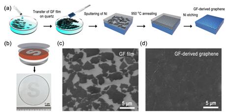
Figure 1. (a) Schematic illustration of the transfer-free synthesis of the GF-derived graphene film on quartz. (b) Simple patterned graphene with the letter “S” on quartz through a desirable mask. Scanning electron microscopy images of (c) well-dispersed GFs and (d) GF-derived graphene.
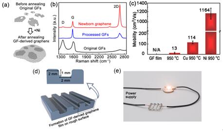
Figure 2. (a) Schematic illustration of structural repair of GFs. (b) Representative Raman spectra of the original GFs, the processed GFs, and newborn graphene. (c) Comparison of the carrier mobility for the GFs with annealing, annealing with Cu, and annealing with Ni at 950 °C. (d) Direct preparation of the GF-derived graphene film on the rough surface of the quartz substrate. (e) Photograph of a continuous GF-derived graphene film on a rough quartz substrate.