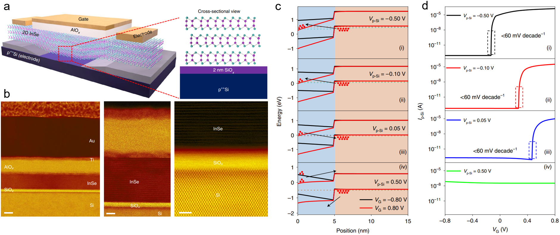
Recently, Weida Hu and Jinshui Miao from the Lab of Infrared Science and Technology of the Shanghai Institute of Technical Physics (SITP) cooperated with D. M. Jariwala made important progress in manipulating tunnel electrons of semiconductor heterojunction by localized electric field. They controlled the energy band of 2D atomic crystals through coupled localized electric fields and achieved effective manipulation of tunnel electrons in InSe/Si semiconductor heterostructures. Their work provides a theoretical and experimental basis for the development of mixed-dimensional heterostructures in high-performance electronic and optoelectronic devices. Their work was published in the journal of Nature Electronics (Heterojunction tunnel triodes based on two-dimensional metal selenide and three-dimensional silicon).
The transport mechanisms of electrons (drift, diffusion, tunneling, etc.) are important to the electronic and optoelectronic devices. In recent years, 2D atomic crystals provide an opportunity to break the performance limits of the electronic and optoelectronic devices due to their adjustable physical properties by localized electric field. However, the electron generation and recombination, tunneling and the mechanism of field manipulation in 2D/3D heterostructure devices are still unclear, and more research of multifunctional devices need to be done.
To solve these problems, the authors studied the transport behavior of tunnel electrons in InSe/Si heterostructures under the coordinated manipulation of gate-voltage and drain-bias. 2D materials show self-passivated surface without dangling bonds and the energy band structure is easily controlled by localized electric field. The band structure of semiconductor heterostructures is controlled by a capacitively-coupled electric field to achieve effective control of electronic band-to-band tunneling efficiency, and negative differential conductance and Zener breakdown are successfully observed. The 2D/3D tunnel triodes show a very low subthreshold swing of 6.4mV/decade and a high current on/off ratio (106).
Prof. Jinshui Miao is the first and corresponding author. D. M. Jariwala is the co-corresponding author.
Contact: jsmiao@mail.sitp.ac.cn

Figure 1. (a) 2D/3D van der Waals heterostructure device (b) cross-section TEM of the heterostructure device (c) 2D/3D energy band manipulated by various electric fields (d) output characteristics curve of the 2D/3D devices.

